- 您现在的位置:买卖IC网 > Sheet目录3890 > PIC18C858T-I/PT (Microchip Technology)IC MCU OTP 16KX16 CAN 80TQFP
PIC18CXX8
DS30475A-page 132
Advanced Information
2000 Microchip Technology Inc.
14.5
PWM Mode
In Pulse Width Modulation (PWM) mode, the CCP1 pin
produces up to a 10-bit resolution PWM output. Since
the CCP1 pin is multiplexed with the PORTC data latch,
the TRISC<2> bit must be cleared to make the CCP1
pin an output.
Figure 14-3 shows a simplified block diagram of the
CCP module in PWM mode.
For a step-by-step procedure on how to set up the CCP
module for PWM operation, see Section 14.5.3.
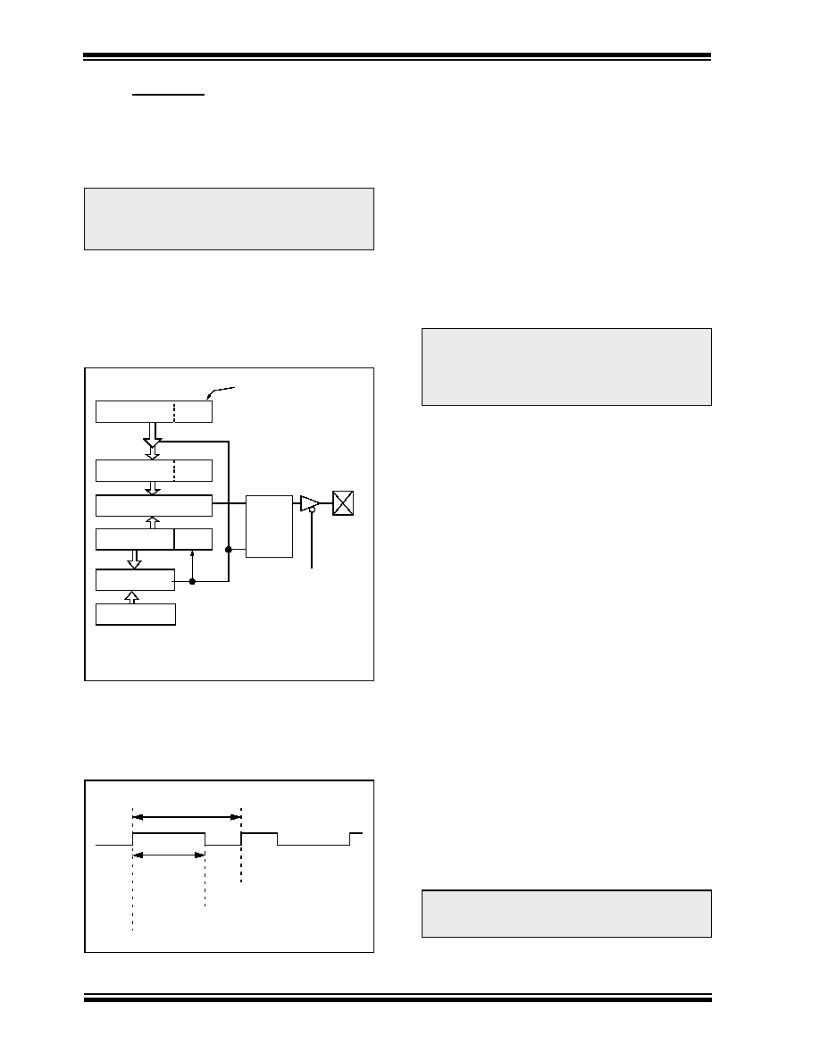
FIGURE 14-3: SIMPLIFIED PWM BLOCK
DIAGRAM
A PWM output (Figure 14-4) has a time-base (period)
and a time that the output stays high (duty cycle). The
frequency of the PWM is the inverse of the period
(1/period).
FIGURE 14-4: PWM OUTPUT
14.5.1
PWM PERIOD
The PWM period is specified by writing to the PR2 reg-
ister. The PWM period can be calculated using the fol-
lowing formula:
PWM period =
[(PR2) + 1] 4 TOSC
(TMR2 prescale value)
PWM frequency is defined as 1 / [PWM period].
When TMR2 is equal to PR2, the following three events
occur on the next increment cycle:
TMR2 is cleared
The CCP1 pin is set (exception: if PWM duty
cycle = 0%, the CCP1 pin will not be set)
The PWM duty cycle is latched from CCPR1L into
CCPR1H
14.5.2
PWM DUTY CYCLE
The PWM duty cycle is specified by writing to the
CCPR1L register and to the CCP1CON<5:4> bits. Up
to 10-bit resolution is available. The CCPR1L contains
the eight MSbs and the CCP1CON<5:4> contains the
two LSbs. This 10-bit value is represented by
CCPR1L:CCP1CON<5:4>. The following equation is
used to calculate the PWM duty cycle in time:
PWM duty cycle =
(CCPR1L:CCP1CON<5:4>)
TOSC (TMR2 prescale value)
CCPR1L and CCP1CON<5:4> can be written to at any
time, but the duty cycle value is not latched into
CCPR1H until after a match between PR2 and TMR2
occurs (i.e., the period is complete). In PWM mode,
CCPR1H is a read-only register.
The CCPR1H register and a 2-bit internal latch are
used to double buffer the PWM duty cycle. This double
buffering is essential for glitchless PWM operation.
When the CCPR1H and 2-bit latch match TMR2, con-
catenated with an internal 2-bit Q clock or 2 bits of the
TMR2 prescaler, the CCP1 pin is cleared.
Maximum PWM resolution (bits) for a given PWM
frequency:
Note:
Clearing the CCP1CON register will force
the CCP1 PWM output latch to the default
low level. This is not the PORTC I/O data
latch.
CCPR1L (Master)
CCPR1H (Slave)
Comparator
TMR2
Comparator
PR2
(Note 1)
R
Q
S
Duty Cycle Registers
CCP1CON<5:4>
Clear Timer,
CCP1 pin and
latch D.C.
TRISC<2>
RC2/CCP1
Note 1:
8-bit timer is concatenated with 2-bit internal Q
clock, or 2 bits of the prescaler, to create 10-bit
time-base.
Period
Duty Cycle
TMR2 = PR2
TMR2 = Duty Cycle
TMR2 = PR2
Note:
The Timer2 postscaler (see Section 12.0)
is not used in the determination of the
PWM frequency. The postscaler could be
used to have a servo update rate at a dif-
ferent frequency than the PWM output.
Note:
If the PWM duty cycle value is longer than
the PWM period, the CCP1 pin will not be
cleared.
FOSC
FPWM
---------------
log
2
()
log
-----------------------------bits
=
发布紧急采购,3分钟左右您将得到回复。
相关PDF资料
PIC18C658T-I/PT
IC MCU OTP 16KX16 CAN 64TQFP
PIC16LC717T-E/SS
IC MCU OTP 2KX14 A/D PWM 20SSOP
PIC16LC771T/SO
IC MCU OTP 4KX14 A/D PWM 20SOIC
PIC16LC771T-E/SO
IC MCU OTP 4KX14 A/D PWM 20SOIC
PIC16C771T-E/SO
IC MCU OTP 4KX14 A/D PWM 20SOIC
PIC16LC770T/SS
IC MCU OTP 2KX14 A/D PWM 20SSOP
PIC16LC717T-I/SO
IC MCU OTP 2KX14 A/D PWM 18SOIC
PIC16LC771T/SS
IC MCU OTP 4KX14 A/D PWM 20SSOP
相关代理商/技术参数
PIC18F1220-E/ML
功能描述:8位微控制器 -MCU 4KB 256 RAM 16 I/O RoHS:否 制造商:Silicon Labs 核心:8051 处理器系列:C8051F39x 数据总线宽度:8 bit 最大时钟频率:50 MHz 程序存储器大小:16 KB 数据 RAM 大小:1 KB 片上 ADC:Yes 工作电源电压:1.8 V to 3.6 V 工作温度范围:- 40 C to + 105 C 封装 / 箱体:QFN-20 安装风格:SMD/SMT
PIC18F1220-E/P
功能描述:8位微控制器 -MCU 4KB 256 RAM 16 I/O RoHS:否 制造商:Silicon Labs 核心:8051 处理器系列:C8051F39x 数据总线宽度:8 bit 最大时钟频率:50 MHz 程序存储器大小:16 KB 数据 RAM 大小:1 KB 片上 ADC:Yes 工作电源电压:1.8 V to 3.6 V 工作温度范围:- 40 C to + 105 C 封装 / 箱体:QFN-20 安装风格:SMD/SMT
PIC18F1220-E/SO
功能描述:8位微控制器 -MCU 4KB 256 RAM 16 I/O RoHS:否 制造商:Silicon Labs 核心:8051 处理器系列:C8051F39x 数据总线宽度:8 bit 最大时钟频率:50 MHz 程序存储器大小:16 KB 数据 RAM 大小:1 KB 片上 ADC:Yes 工作电源电压:1.8 V to 3.6 V 工作温度范围:- 40 C to + 105 C 封装 / 箱体:QFN-20 安装风格:SMD/SMT
PIC18F1220-E/SS
功能描述:8位微控制器 -MCU 4KB 256 RAM 16 I/O RoHS:否 制造商:Silicon Labs 核心:8051 处理器系列:C8051F39x 数据总线宽度:8 bit 最大时钟频率:50 MHz 程序存储器大小:16 KB 数据 RAM 大小:1 KB 片上 ADC:Yes 工作电源电压:1.8 V to 3.6 V 工作温度范围:- 40 C to + 105 C 封装 / 箱体:QFN-20 安装风格:SMD/SMT
PIC18F1220-H/ML
功能描述:8位微控制器 -MCU 4KB FL 256RAM 16 I/O RoHS:否 制造商:Silicon Labs 核心:8051 处理器系列:C8051F39x 数据总线宽度:8 bit 最大时钟频率:50 MHz 程序存储器大小:16 KB 数据 RAM 大小:1 KB 片上 ADC:Yes 工作电源电压:1.8 V to 3.6 V 工作温度范围:- 40 C to + 105 C 封装 / 箱体:QFN-20 安装风格:SMD/SMT
PIC18F1220-H/P
功能描述:8位微控制器 -MCU 4KB FL 256RAM 16 I/O RoHS:否 制造商:Silicon Labs 核心:8051 处理器系列:C8051F39x 数据总线宽度:8 bit 最大时钟频率:50 MHz 程序存储器大小:16 KB 数据 RAM 大小:1 KB 片上 ADC:Yes 工作电源电压:1.8 V to 3.6 V 工作温度范围:- 40 C to + 105 C 封装 / 箱体:QFN-20 安装风格:SMD/SMT
PIC18F1220-H/SO
功能描述:8位微控制器 -MCU 4KB FL 256RAM 16 I/O RoHS:否 制造商:Silicon Labs 核心:8051 处理器系列:C8051F39x 数据总线宽度:8 bit 最大时钟频率:50 MHz 程序存储器大小:16 KB 数据 RAM 大小:1 KB 片上 ADC:Yes 工作电源电压:1.8 V to 3.6 V 工作温度范围:- 40 C to + 105 C 封装 / 箱体:QFN-20 安装风格:SMD/SMT
PIC18F1220-H/SS
功能描述:8位微控制器 -MCU 4KB FL 256RAM 16 I/O RoHS:否 制造商:Silicon Labs 核心:8051 处理器系列:C8051F39x 数据总线宽度:8 bit 最大时钟频率:50 MHz 程序存储器大小:16 KB 数据 RAM 大小:1 KB 片上 ADC:Yes 工作电源电压:1.8 V to 3.6 V 工作温度范围:- 40 C to + 105 C 封装 / 箱体:QFN-20 安装风格:SMD/SMT